

- RFQ
- BOM
-
Contact Us
Tel: +86-0755-83501315
Email: sales@sic-components.com


- Chinese
- English
- French
- German
- Portuguese
- Spanish
- Russian
- Japanese
- Korean
- Arabic
- Irish
- Greek
- Turkish
- Italian
- Danish
- Romanian
- Indonesian
- Czech
- Afrikaans
- Swedish
- Polish
- Basque
- Catalan
- Esperanto
- Hindi
- Lao
- Albanian
- Amharic
- Armenian
- Azerbaijani
- Belarusian
- Bengali
- Bosnian
- Bulgarian
- Cebuano
- Chichewa
- Corsican
- Croatian
- Dutch
- Estonian
- Filipino
- Finnish
- Frisian
- Galician
- Georgian
- Gujarati
- Haitian
- Hausa
- Hawaiian
- Hebrew
- Hmong
- Hungarian
- Icelandic
- Igbo
- Javanese
- Kannada
- Kazakh
- Khmer
- Kurdish
- Kyrgyz
- Latin
- Latvian
- Lithuanian
- Luxembou..
- Macedonian
- Malagasy
- Malay
- Malayalam
- Maltese
- Maori
- Marathi
- Mongolian
- Burmese
- Nepali
- Norwegian
- Pashto
- Persian
- Punjabi
- Serbian
- Sesotho
- Sinhala
- Slovak
- Slovenian
- Somali
- Samoan
- Scots Gaelic
- Shona
- Sindhi
- Sundanese
- Swahili
- Tajik
- Tamil
- Telugu
- Thai
- Ukrainian
- Urdu
- Uzbek
- Vietnamese
- Welsh
- Xhosa
- Yiddish
- Yoruba
- Zulu
- Kinyarwanda
- Tatar
- Oriya
- Turkmen
- Uyghur
Pcb Layout: Everything you need to know
PCB layout—it’s not exactly rocket science, but it’s way trickier than it looks. It’s that crucial step where your electronic design goes from paper to something real. Whether the circuit works properly, the signals stay clean, or it resists interference—all that depends on how well you handle this part. Seriously, mess up the layout, and even the fanciest phone motherboard or industrial module will lose half its performance. No joke.
You gotta prep before diving in; set the rules right, and things go smoother later. Stack - up design is a big deal. For high - speed circuits, 4 - layer boards are common: top and bottom layers for signals, middle layers for ground and power. This way, the power stays stable, signal return paths are smooth, and radiation is kept in check. For low - speed, low - frequency stuff, 2 - layer boards can get by, but power and ground lines need to be thick and short. Don’t let them loop around, or noise will flood in like crazy.
Picking the right component packages matters too. SMD parts save space compared to through - hole ones. 0402 resistors and capacitors are smaller than 0805s, but hand - soldering them can be a nightmare. For components in high - frequency signal paths, go for packages with short leads, like QFN or LGA—they have less parasitic inductance. Take RF circuit crystals, for example; HC - 49SMD is way better than the traditional DIP type. I’ve tested it, and it cuts phase noise by 30%.
Design rules need to be set beforehand. Line width depends on current. With 1oz copper, a 1mm wide line can handle about 1A. Power main lines should be at least 2mm to be reliable. Spacing isn’t random either. For 220V high voltage, it needs to be at least 0.5mm. High - speed differential pairs, like USB 3.0, need controlled impedance around 90Ω, with spacing usually between 0.15 and 0.2mm. A little off, and problems pop up.
Component placement is all about grouping by function. Power, digital, analog, and high - frequency sections should each have their own space—don’t mix them up. In a microcontroller system, put the MCU in the middle, with the crystal and reset circuit right next to it. Power modules like LDOs and DC - DCs should be close to the load to reduce line loss.
RF modules, say WiFi chips, must be kept far from digital circuits. Otherwise, digital noise will mess up the wireless signal—learned that the hard way. Sensitive components need extra care. Op - amp inputs should be at least 5cm away from “noise sources” like power inductors and switching transistors, or the signal gets contaminated instantly.
The crystal and its load capacitors must be glued to the MCU’s clock pins. If the line length exceeds 3mm, stray capacitance creeps in, the clock jitters badly, and the program might even crash. In analog circuits, the reference voltage VREF needs a separate trace. Don’t run it parallel to digital lines; better to wrap it with a ground “guard band”—super stable, trust me.
Heat dissipation is another thing. Power devices like MOSFETs and LDOs should be placed near the PCB edges or heat vias. For high - current areas, thicken the copper and add more vias to connect to the bottom heat plane. A 1W LDO in a 25°C environment? If the copper area is less than 10cm², the temperature can shoot over 125°C—might even burn out.
Routing is like traffic control for signals; keep them flowing smoothly. Ground is the top priority. Analog and digital grounds should connect at a single point—maybe through a 0Ω resistor or a bead—star - shaped grounding. Otherwise, noise from the digital ground will leak into the analog circuit, ruining the analog signal.
For high - frequency signals above 100MHz, the return path must be parallel and close to the signal path. Use the ground plane as the return channel; the smaller the loop area, the better. It’s the golden rule for EMI suppression—ignore it, and you’ll regret it.
High - speed differential pairs, such as USB and HDMI, need equal length and spacing, and impedance matching. Try to route them straight; if you have to turn, use 45 - degree angles, not right angles—impedance jumps are deadly. For DDR4 differential clock pairs, the length error can’t exceed ±5mil, or the timing goes haywire. If you have to snake the lines to match lengths, don’t stick vias or components between the differential pair—it’s really bad.
Power routing has its order. Main power lines like 5V and 3.3V need to be thick, with multiple power points. Right next to an IC’s power pin, there must be decoupling capacitors—a 100nF ceramic one plus a 10μF electrolytic one. Keep them tight to the pin, with traces no longer than 2mm. These caps act like little reservoirs, soaking up current spikes during switching.
For sensitive analog power, like an ADC’s AVDD, stick an LC filter at the input—a 10μH inductor plus a 100nF capacitor. It’ll filter out most high - frequency noise.
Going a step further, EMC and reliability need work. Don’t punch big holes in the ground plane. A hole over 5mm in diameter might break the signal return path. Clock lines and high - speed buses like SPI and I2C should be as short as possible. For long distances, add termination resistors. A 1 - meter CAN bus with a 120Ω resistor in parallel? It cuts down reflections a lot.
If radiation is too high, slip a ferrite bead over key signal lines. Add a grounded copper strip around the PCB edge as a “shield ring”—absorbs edge radiation, works pretty well.
Reliability is in the details. In humid environments, cover all PCB areas except pads with solder mask, or the copper will oxidize. For car electronics that vibrate a lot, pick components with mounting holes—like QFPs with heat sinks. Secure them with vias. Leave plenty of test points: power, clock, reset—all the important signals. Make them at least 0.8mm in diameter, 2mm apart. Trust me, you’ll thank yourself when debugging; otherwise, you’ll be tearing your hair out.
Newbies fall into so many traps. Stick high - power components next to precision sensors? The sensor gets so much interference it stops working. Forget to check component heights? Then you’ll find the case won’t close when assembling. Put fine - pitch QFPs (0.5mm pitch) on the PCB edge? Screen printing becomes a nightmare, and you’ll end up with all sorts of cold solder joints.
High - speed signals have sneakier pitfalls. When the rate goes over 1Gbps, regular routing won’t cut it. Take PCIe 4.0—you need impedance matching and crosstalk prevention. Adjacent lines must be at least 3 times the line width apart.
Don’t underestimate vias. One via adds about 0.5pF of parasitic capacitance. On high - speed signal paths, use no more than two vias. If you use more, you gotta fire up simulation software like Cadence Allegro to check signal integrity. Otherwise, you’ll never figure out what went wrong.
All in all, there’s no “perfect” PCB layout—just the best fit for the job. Balance area, performance, and cost. Low - speed circuits don’t need over - engineering; just make them manufacturable. But for high - speed, precision stuff, sweat the details. A 0.1mm difference in line width can mess things up. Every layout revision teaches you more about circuit theory. Those traces under the copper? They’re the real “invisible backbone” of the electronic world. If you get it, you get it.
https://www.sic-components.com/

Hot Products
View More-
DRV5056A4ELPGMQ1 Texas Instruments
-
A1302ELHLT-T Allegro MicroSystems
-

HMC1021S-TR Honeywell Aerospace
-
MLX90290LSE-AAA-520-SP Melexis Technologies NV
-
MLX90393SLW-ABA-012-SP Melexis Technologies NV
-
DRV5056A1ELPGQ1 Texas Instruments
-

ACS37600KOKATN-006B5-C Allegro MicroSystems
-
TLE4998C3CHAMA1 Infineon Technologies
-
MLX90333LDC-BCH Melexis Technologies NV
-
91SS12-2 Honeywell Sensing and Productivity Solutions
-

MLX90397RLQ-AAA-000-SP Melexis Technologies NV
-
MLX90290LSE-AAA-310-SP Melexis Technologies NV
Related Blogs
-
2025 / 07 / 19
Broadcom BCM5714CKPB: Featrues,Applications,Datasheet And Advantages
When it comes to reliable, high-performance network connectivity in enterprise and industrial systems, the Broadcom BCM5714CKPB stands as a standout solution. This dual-port Gigabit Ethernet controller, developed by Broadcom—a leader in semiconductor innovation—combines robust features, versatile co...

-
2025 / 07 / 15
MC7447AHX1000NB: Technical Analysis and Applications of a High-Performance PowerPC Architecture Proc
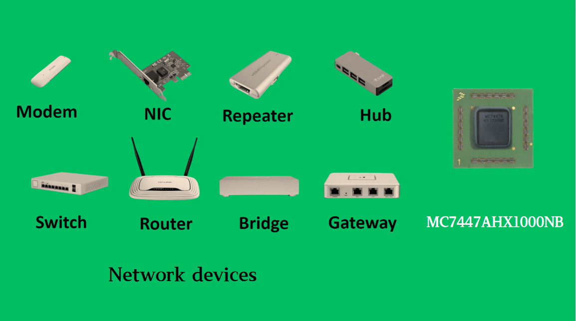
In the field of embedded computing and network systems, the performance, energy efficiency, and compatibility of processors are often crucial to the success of a design. The MC7447AHX1000NB launched by NXP (formerly Freescale), as an important member of the MPC7447A series, has become an ideal choic...
-
2025 / 07 / 14
Nexperia Unveils New 1200V/20A SiC Schottky Diodes to Empower Efficient Industrial Power Innovations
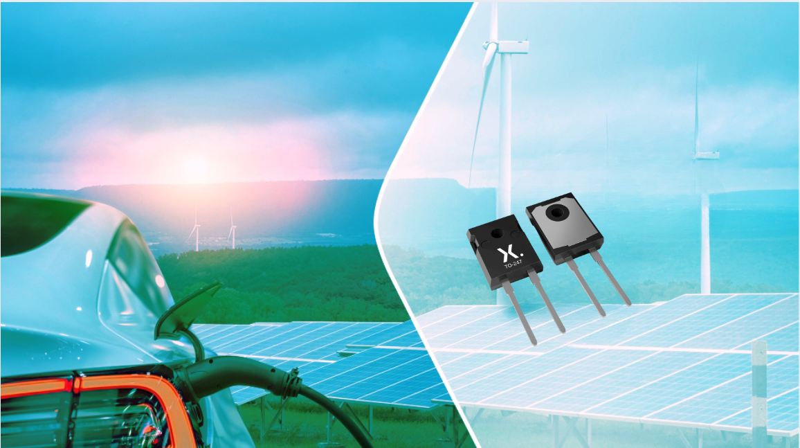
Nexperia recently announced the addition of two new 1200V, 20A silicon carbide (SiC) Schottky diodes—PSC20120J and PSC20120L—to its power electronics portfolio, further expanding its product landscape in high-performance semiconductors. Specifically designed to address the increasingly stringent dem...
-
2025 / 07 / 09
CD4007: A Comprehensive Analysis of a Multifunctional CMOS Integrated Circuit
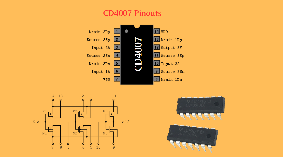
In the field of modern electronic technology, CMOS (Complementary Metal-Oxide-Semiconductor) integrated circuits have become core components in digital and analog circuit design due to their low power consumption, high integration, and excellent compatibility. As a classic CMOS device, the CD4007 oc...
-
2025 / 07 / 07
Understanding IC 7408: A Fundamental Component in Digital Logic Design
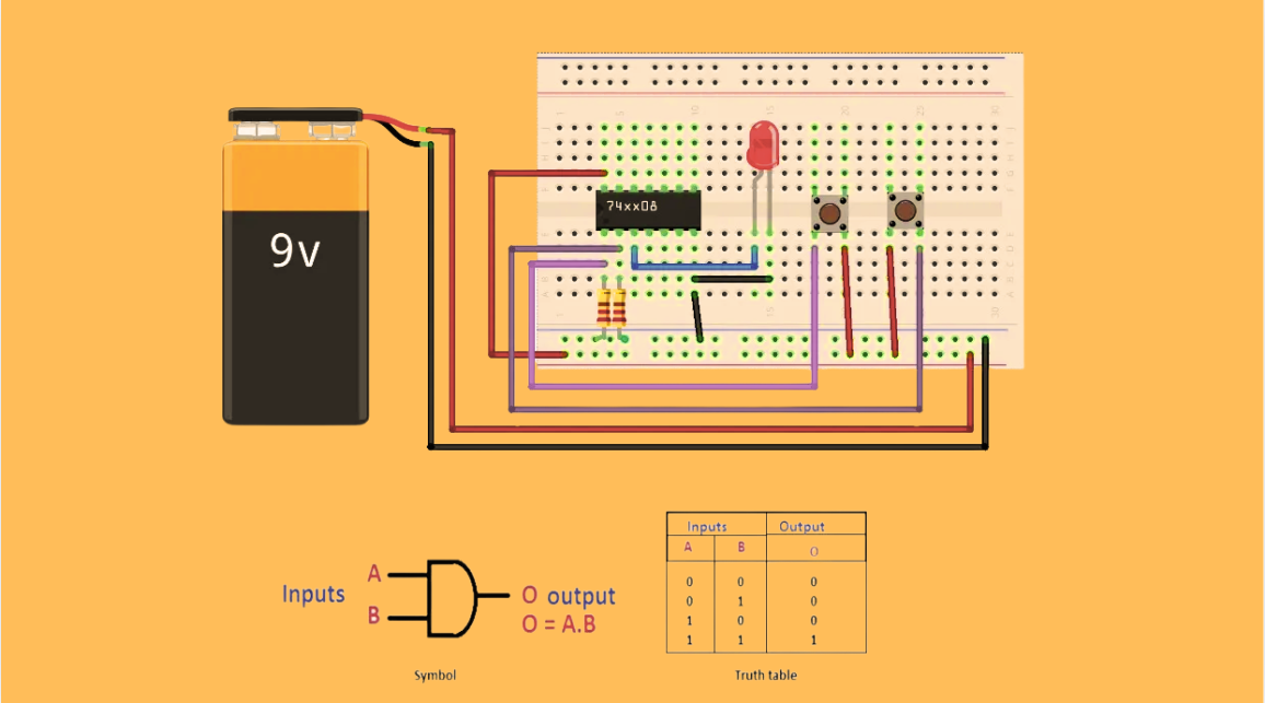
In the vast and intricate realm of digital electronics, integrated circuits (ICs) serve as the building blocks that enable the creation of complex and powerful systems. Among these, the IC 7408 holds a special place as a fundamental component in digital logic design. This article aims to provide a c...
-
2025 / 07 / 04
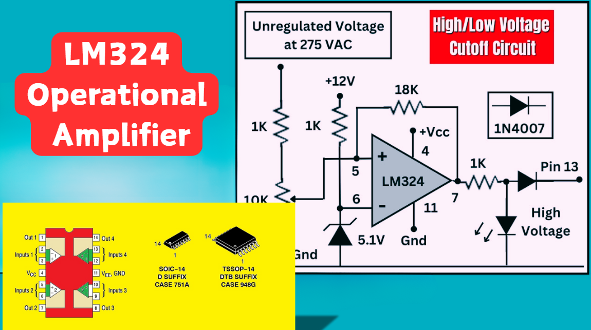
LM324 Operational Amplifier Comprehensive Guide: Pins, Applications, Packaging, and Datasheet
The LM324 is a low-cost integrated circuit featuring four independent operational amplifiers (op-amps), renowned for its wide voltage adaptability, low power consumption, and high reliability in industrial and consumer electronics. With a single-supply voltage range of 3V to 32V (or dual-supply rang...
-
2025 / 07 / 02
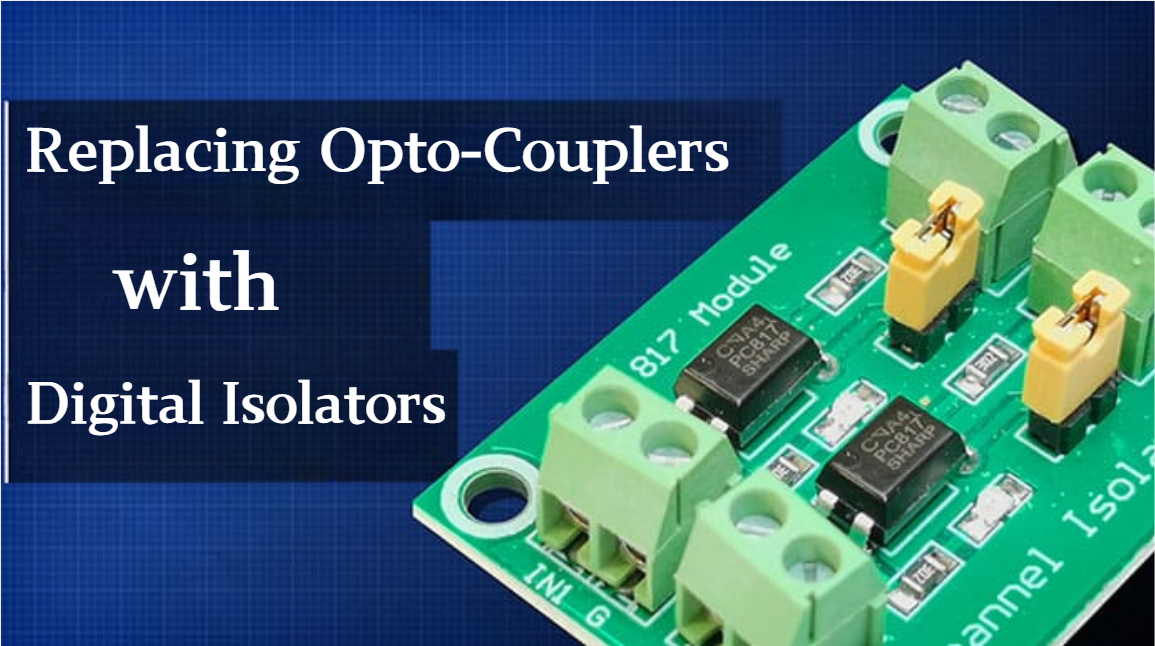
A Comprehensive Guide to Replacing Opto-Couplers with Digital Isolators: From Principles to Practice
In the ever-evolving landscape of electronic design, the transition from opto-couplers to digital isolators marks a pivotal shift in isolation technology. For decades, opto-couplers have been the cornerstone of electrical isolation in industrial control, medical devices, and power systems, relying o...
-
2025 / 06 / 30
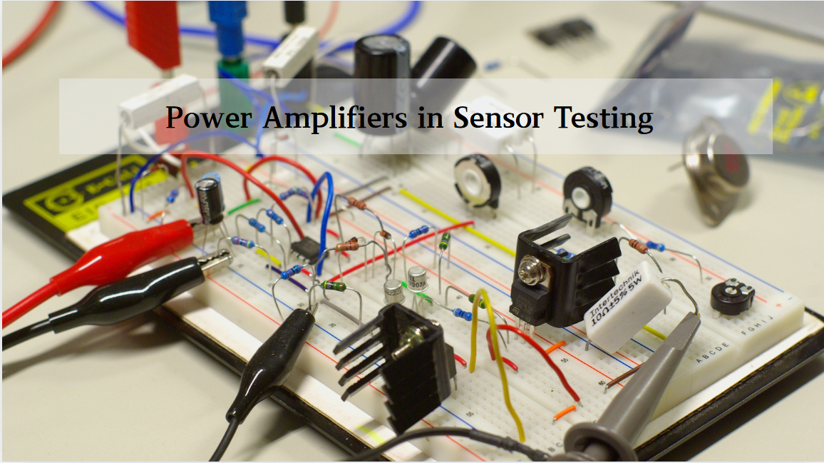
Multivariate Application Analysis of Power Amplifiers in Sensor Testing
In the field of modern sensor testing, power amplifiers (PAs) serve as core components and play an indispensable role. From amplifying weak signals to simulating complex physical environments, power amplifiers provide solid guarantees for the precise testing of sensor performance through their uniqu...
-
2025 / 06 / 28
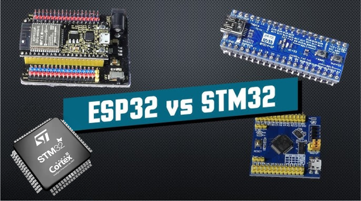
ESP32 vs STM32: Which Microcontroller Suits You Better?
In the field of embedded development, both ESP32 and STM32 are highly favored microcontrollers, each with unique features and advantages. When facing project development, how do you choose between them? This requires comprehensive consideration of multiple factors. The following detailed comparison ...
-
2025 / 06 / 26
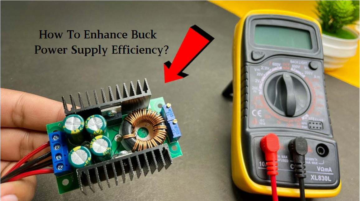
Key Strategies to Enhance Buck Power Supply Efficiency
Improving the efficiency of Buck (step-down) switching power supplies requires a multi-dimensional approach targeting energy loss sources, including component selection, topology optimization, control strategies, and thermal management. Below are core strategies and engineering practices:...

2000+
Daily average RFQ Volume

30,000,000
Standard Product Unit

2800+
Worldwide Manufacturers

15,000 m2
In-stock Warehouse
 Wishlist (0 Items)